
Wireless Power (C)


This was the project that won the 2015 CT Junior Science and Humanities Symposium. I was a junior in high school. If you’d like to read more about the technical details of the project, you can read the paper I submitted at the time. Here, I’d like to show more of the pictures of the set up and other documentation that wouldn’t go in a paper.
At the time, inductive wireless charging was really becoming mainstream. However, the TX and RX coils of the system were bulky, needed precise alignment, and were costly, With phones getting bigger and bigger, what if we used the body of the phone as the plate of a capacitor, and capacitively coupled the TX and RX? It’s the same principle of resonance, but a series RC circuit instead of a parallel RC one. Seemed like a good science project to me. I had access to a lab because of the ARM (Advanced Research Mentorship) Program at school, and I had access to all the papers I could need via UCONN, though there was little literature on this subject. The main reason I felt qualified to tackle this project was my experience in resonance circuits, H-bridges and half bridges, and gate drivers. Half a decade of high voltage and tesla coil work had paid off.

Remarks on Circuit
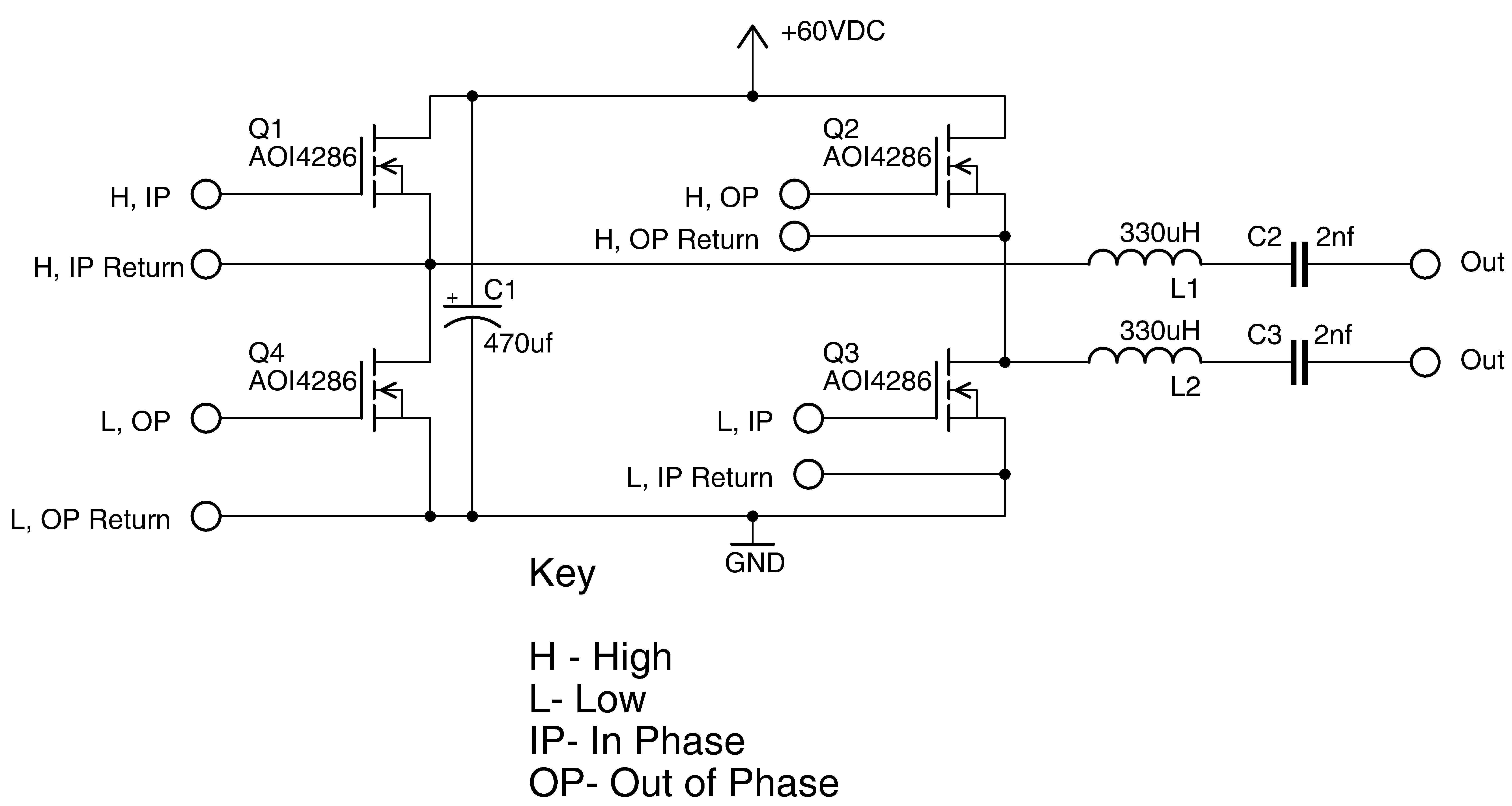
Basic idea is pretty simple. Drive a series LC circuit as resonance, and couple power from the source to load at maximum efficiency and minimum impedance. Of course there can’t be a wire for the return, so there are two sets of series LC circuits.
The AC source is an H or half bridge driven by a frequency source at the tank resonance. This is implemented fairly straightforwardly with the IR2113 gate drivers. The bridge MOSFTs were chosen for extremely low RdsON losses, in addition to general high performance. Since there are two series LC circuits in series, the resonance frequency was 200kHz. (1nF and 660uH
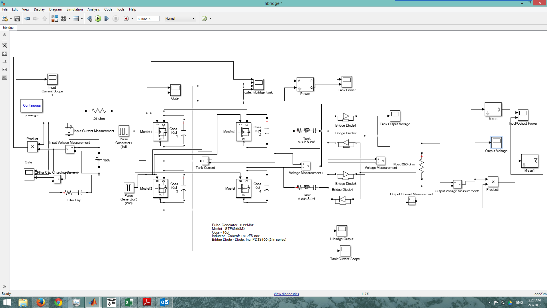

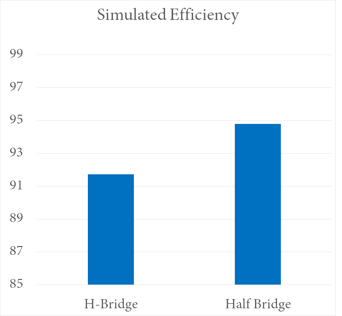
The science fair wasn’t really geared towards engineering projects like this, so I had to have a traditional hypothesis. So, I decided to test to see if there was a difference between H-bridge and half bridge topologies in this applications. In truth, I’m not sure it made a whole lot of difference. I first did some testing in Simulink. Yup, at resonance current and voltage are in phase. Not sure how relevant my simulated efficiency is.
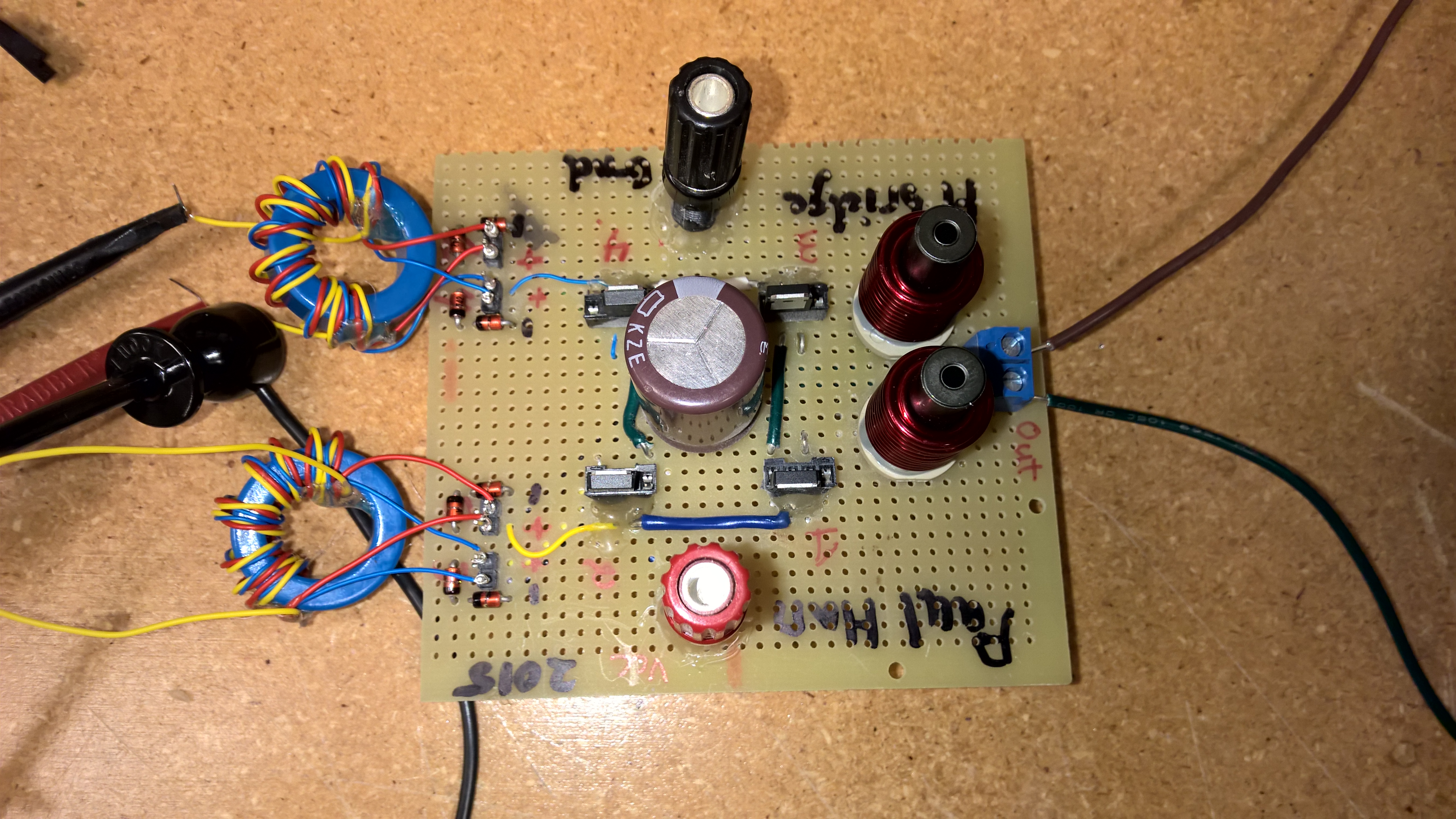

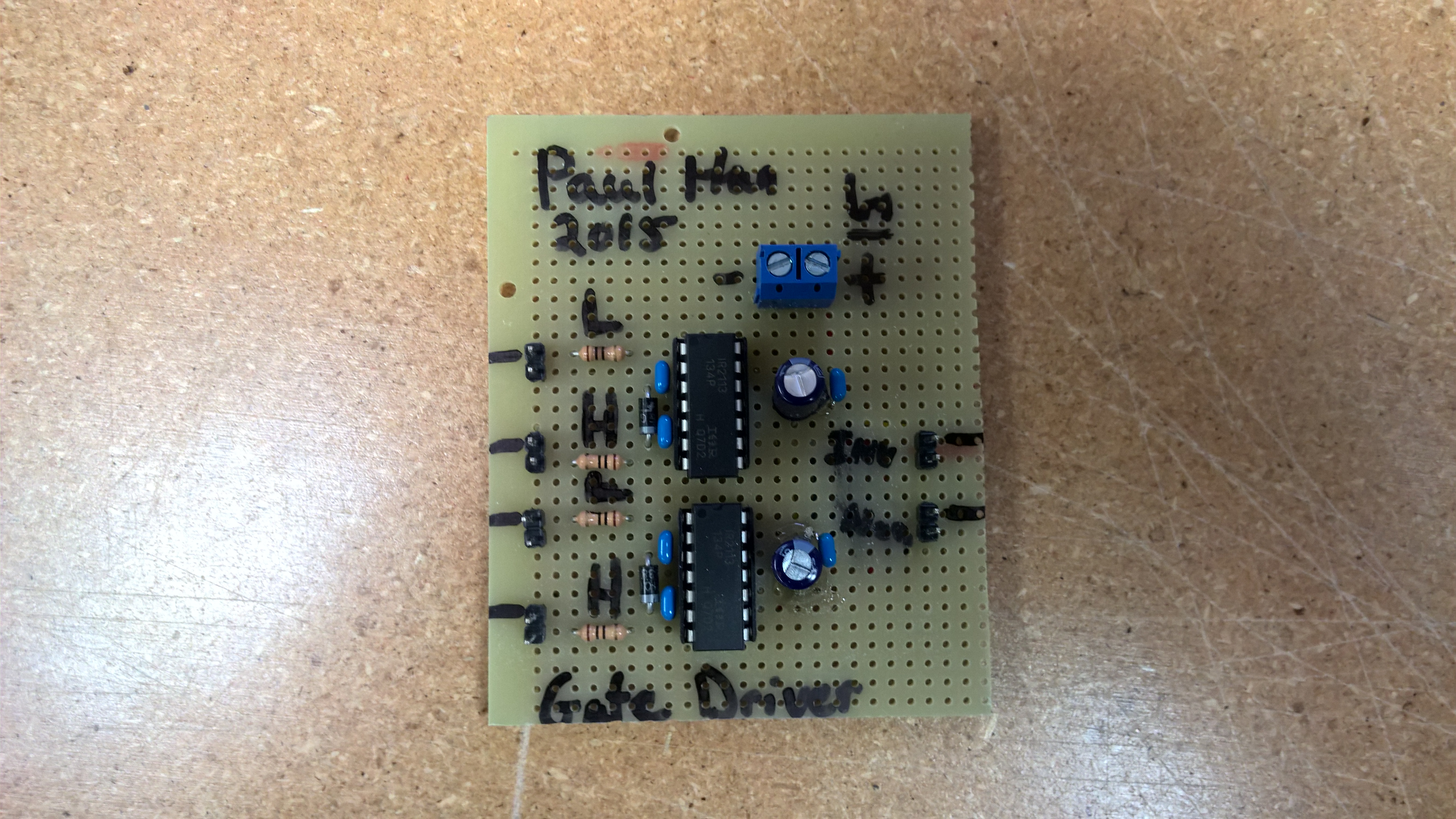

I didn’t have time to wait for PCBs to be manufactured, so this 200kHz RF circuit was built using through hole and perf board technology. Not exactly ideal. You can see my hand wound gate drive transformers in the first picture. They actually worked really well, eBay ferrite cores and all! Beat the pants off the commercial samples I ordered.
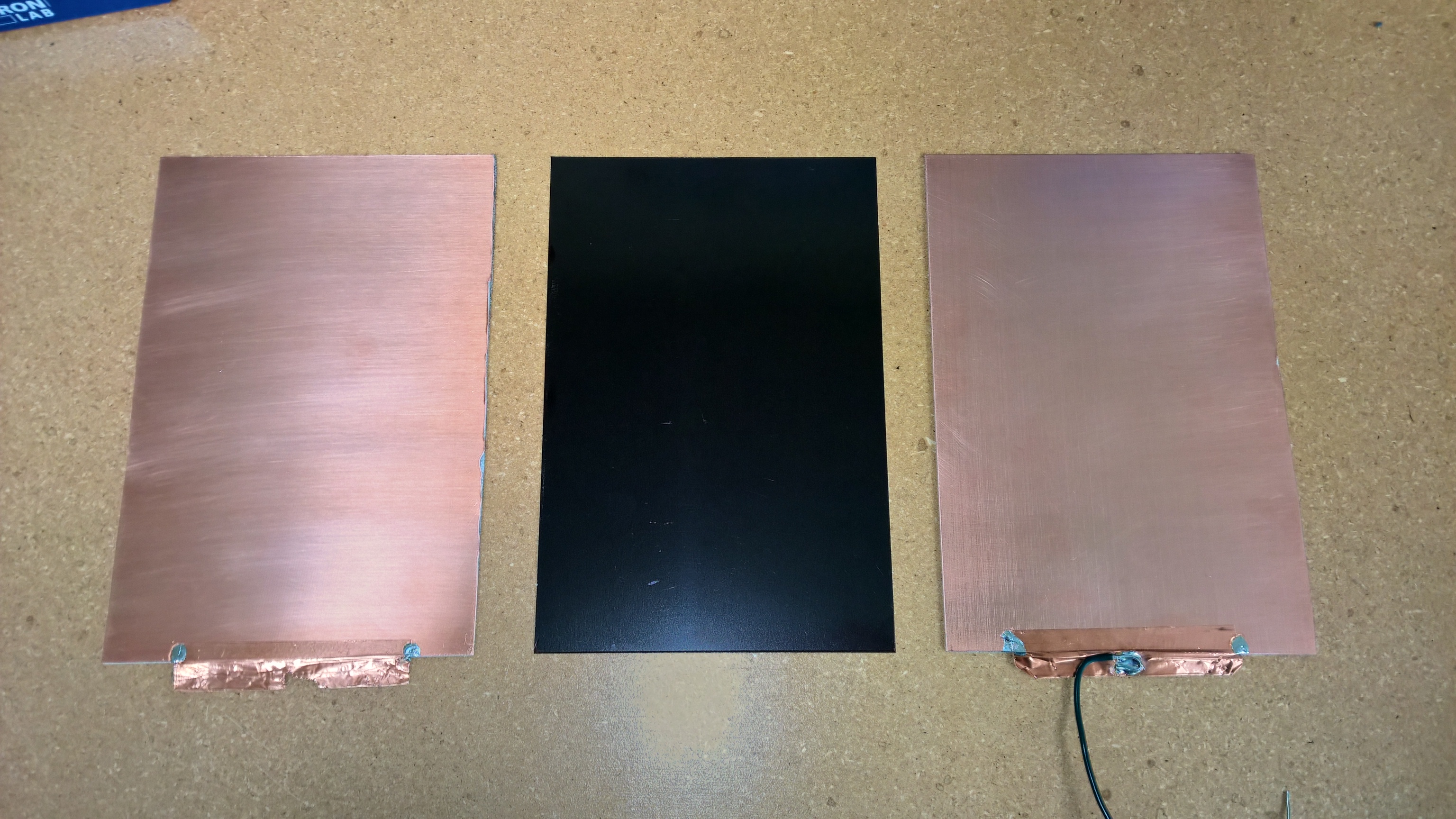

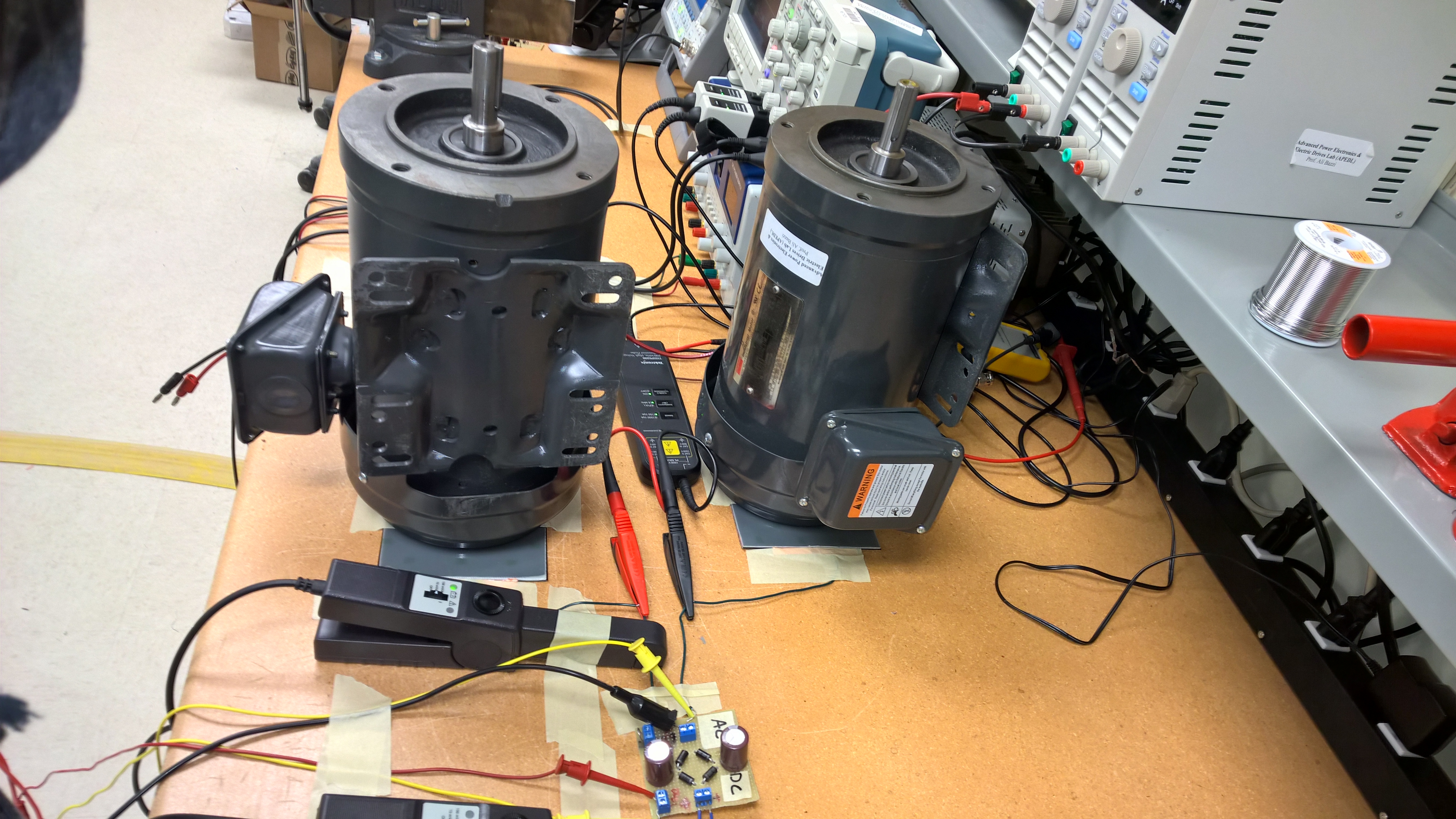
My designed aimed for about 2nf of capacitance for these air capacitors. I used Kapton sheets for their high dielectric constant to achieve that figure. These capacitors, made out of PC board, copper tape, and Kapton, were 2nf on the nose. Of course, one of the drawbacks of my system is that the plates had to be extremely close to each other to maintain even a tiny amount of capacitance like 2nf. That’s why I ended up using induction motors to really sandwich the two together. Perhaps a sign this system wouldn’t be the most practical commercially.

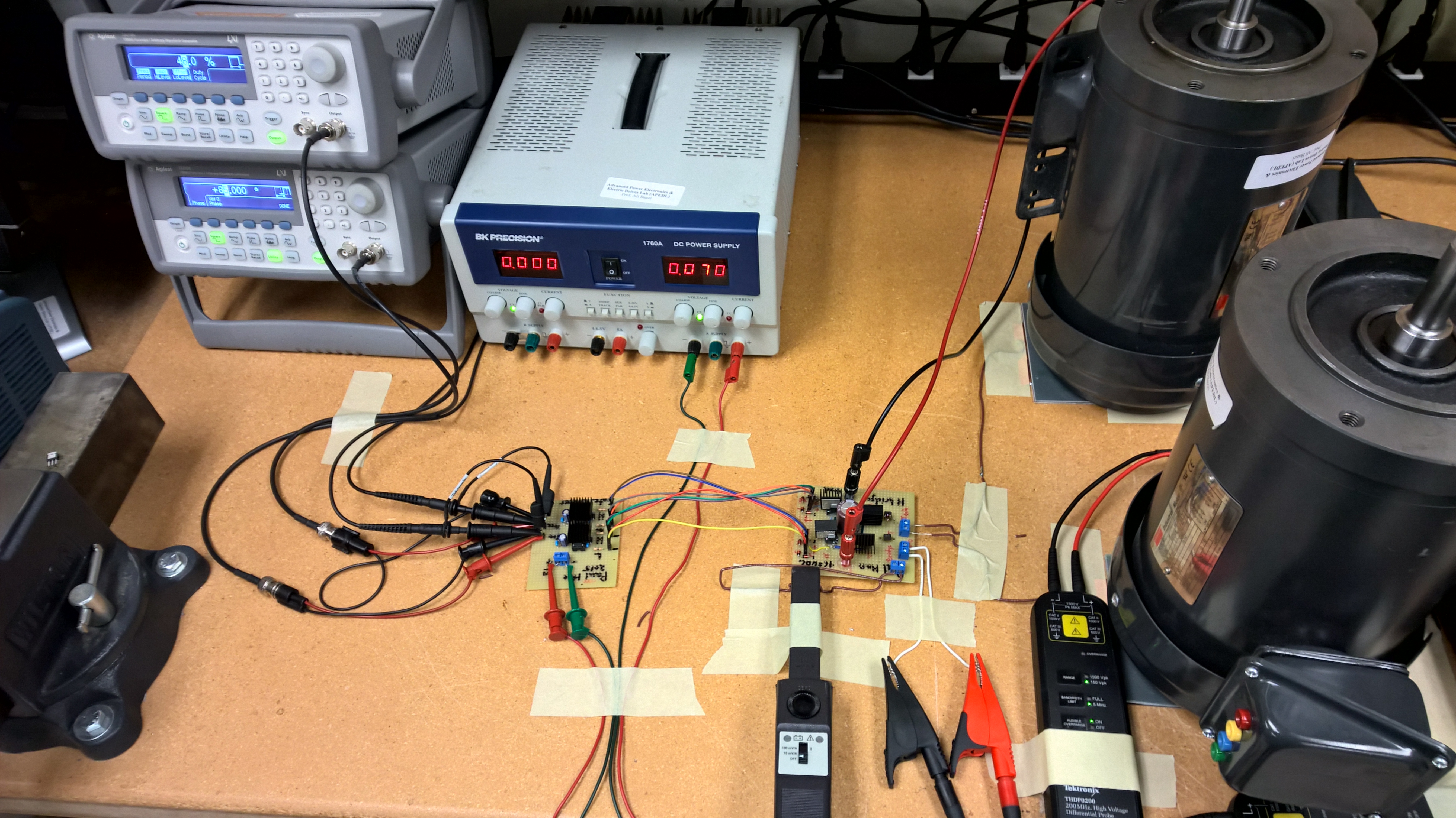

Here’s the set up, in all of its masking tape glory. I’m very thankful that I had access to a lab at the time. While I didn’t receive much guidance, I did get to use all the equipment. In this picture is probably $30,000 of equipment. Tek current probes are expensive!
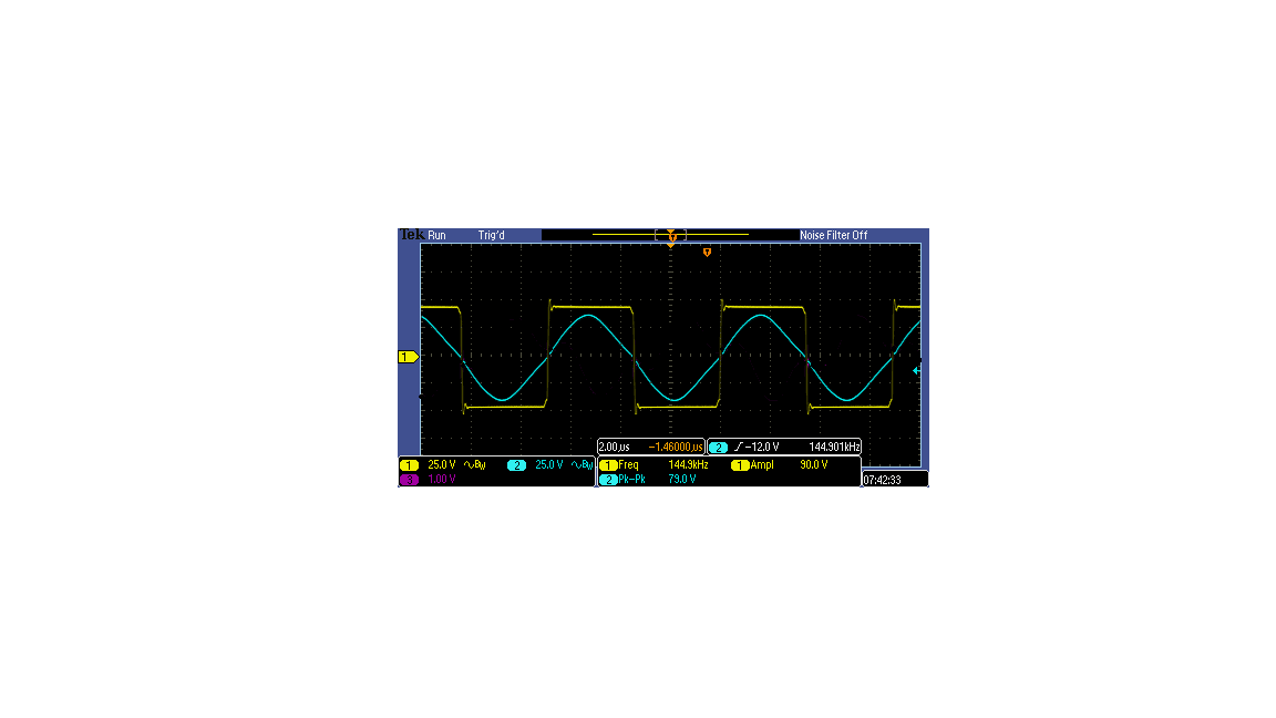

Here is gate drive, tank voltage, and tank current. Sorry I don’t have better screen captures, read the paper if you want more details.
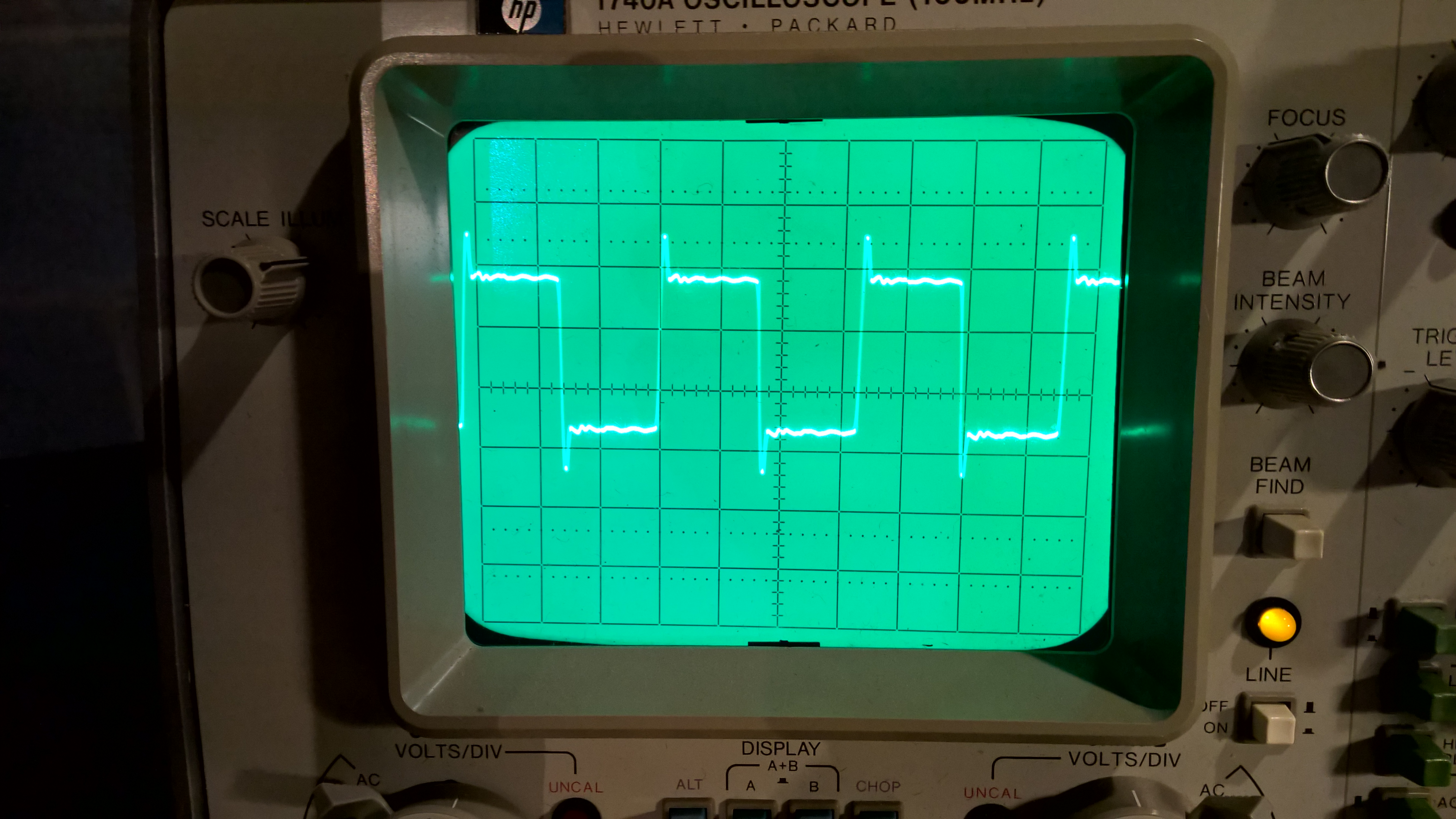
I do have this wonderfully sharp trace of gate driver output on my HP 1740A oscilloscope. Just wanted to show it.
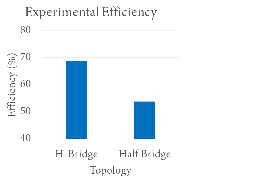
The pictures of the boards I’ve shown you above are actually not what was used in final testing. I switched out the inductors and for the half-bridge used PP film capacitors, I believe. However, I still think the reason the Half bridge performed so much worse was the poor RF performance of the capacitors I used.
