
Wireless Power (GaN)
The Wireless Power that Never Was

After winning JSHS, my mentor (Dr. Bazzi) asked me to work on the next step of the project, which was designing a real demo unit, PCB and SMD and all. One thing he was keen on was using GaN MOSFETs in the bridges, for better RF performance and lower losses. I was really excited about this, so I went about redesigning the whole system to use high performance components. I even added a Buck-Boost converter based on an LT chip (RIP in Peace) to the receiver stage. Much of the circuity was designed using the datasheet examples for the individual components. Choosing components was easy due to scarcity – there wasn’t much on the market for GaN at the time.
Remarks on Circuit
The PowerPoint attached shows our progress in October of 2015 and doesn’t show my final schematic and component selection. I finished my schematic and board by December. The schematics don’t show my GaN device selection. After many days and dozens of hours of comparing the devices available at the time, I chose the EPC2001 devices. I’m sure there are much better ones now.
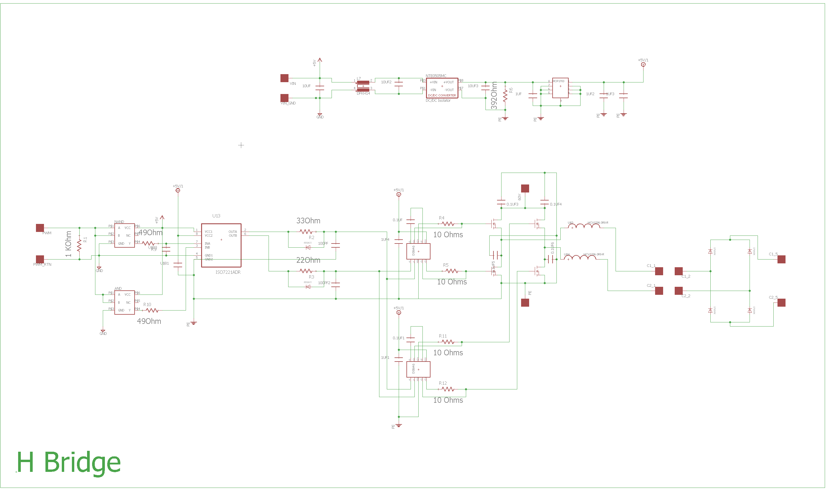
The circuit is fairly straightforward, with AND and NAND gates for in phase and out of phase drive signals, an optical isolater, gate drive chips, and the bridge circuits. The diode resistor and capacitor ensure minimum deadtime between transistor switching. It is meant to be driven using a single signal generator source.


Unfortunately, when I finished designing the board I was told by Dr. Bazzi that his funding was cut, so my project was being scrapped. A real shame.
